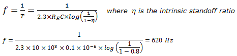
Friends, I am mentioning here some good books for GATE, ISRO, PSUs and for all type of competitive exams. These books are really very nice theoretically and conceptually. Among them some of are my favorite also. I have also given the pictures of their cover page so that it will be easy for you to recognize the books.
FOR ANALOG ELECTRONICS
 Title: Electronic Devices and Circuit Theory, 9th Edition
Author: Robert L. Boylestad, Louis Nashelsky
Publication: Pearson
Contents: Diodes, Diode applications, BJT, DC Biasing-BJT, BJT AC Analysis, FET, FET Biasing, FET Amplifier, BJT & FET frequency response, Operational Amplifier, Power Amplifier, Linear-Digital ICs, Feedback & Oscillator circuits, Power Supplies (Voltage Regulators), Other two terminal devices, pnpn and other devices
FOR DIGITAL ELECTRONICS
FOR ANALOG ELECTRONICS
Author: Robert L. Boylestad, Louis Nashelsky
Publication: Pearson
Contents: Diodes, Diode applications, BJT, DC Biasing-BJT, BJT AC Analysis, FET, FET Biasing, FET Amplifier, BJT & FET frequency response, Operational Amplifier, Power Amplifier, Linear-Digital ICs, Feedback & Oscillator circuits, Power Supplies (Voltage Regulators), Other two terminal devices, pnpn and other devices
FOR DIGITAL ELECTRONICS

Title: Digital Design, 4th Edition
Author: M. Morris Mano, Michael D. Ciletti
Publication: Pearson
Contents: Digital Systems and Binary Numbers, Boolean Algebra and Logic Gates, Gate-Level Minimization, Combinational Logic, Synchronous Sequential Logic, Registers and Counters, Memory and Programmable Logic, Design at the Register Transfer Level, Asynchronous Sequential Logic, Digital Integrated Circuits, Laboratory Experiments with Standard ICs and FPGAs, Standard Graphic Symbols
FOR VLSI

Title: CMOS Digital Integrated Circuits Analysis and Design, 3rd Edition
Author: Sung-Mo Kang, Yusuf Leblebici
Publication: TATA McGraw-Hill
Contents: Fabrication of MOSFETS, MOS Transistor, Modeling of MOS Transistors using SPICE, MOS Inverters: Static Characteristics, MOS Inverters: Switching Characteristics and Interconnect Effects, Combinational MOS Logic Circuits, Sequential MOS Logic Circuits, Dynamic Logic Circuits, Semiconductor Memories, Low-Power CMOS Logic Circuits, BICOMS Logic Circuits, Chip Input and Output Circuits, Design for Manufacturability, Design for Testabililty
FOR COMMUNICATION SYSTEM

Title: Principles of Communication Systems, 3rd Edition
Author: Herbert Taub, Donald Schilling, Goutam Saha
Publication: TATA McGraw-Hill
Contents: Introduction: Signal and Spectra, Random variables and Processes, Amplitude-Modulation Systems, Angle Modulation, Pulse Modulation and Digital Transmission of Analog Signal, Digital Modulation and Transmission, Mathematical Representation of Noise, Noise in Amplitude Modulation System, Noise in Frequency Modulation Systems, Phase Locked Loops, Optimal Reception of Digital Signal, Noise in Pulse Code Modulation and Delta Modulation Systems, Information Theory and Coding, Communication Systems and Component Noises, Spread Spectrum Modulation
FOR ELECTROMAGNETIC THEORY

Title: Electromagnetic Field Theory Fundamentals, 2nd Edition
Author: Bhag Singh Guru, Hüseyin R. Hiziroglu
Publication: Cambridge University Press
Contents: Electromagnetic Field Theory, Vector Analysis, Electrostatics, Steady Electric Currents, Magnetostatics, Application of static fields, Time-varying Electromagnetic Fields, Plane Wave Propagation, Waveguides and Cavity Resonators, Antennas, Computer-aided Analysis of Electromagnetic Fields
FOR MICROWAVE ENGINEERING

Title: Microwave Engineering, 3rd Edition
Author: David M. Pozar
Publication: Wiley India
Contents: Electromagnetic Theory, Transmission Line Theory, Transmission Lines And Waveguides, Microwave Network Analysis, Impedance Matching And Tuning, Microwave Resonators, Power Dividers And Directional Couplers, Microwave Filters, Theory And Design Of Ferrimagnetic Components, Noise And Active Rf Components, Microwave Amplifier Design, Oscillators And Mixers
FOR DIGITAL SIGNAL PROCESSING

Title: Digital Signal Processing, 4th Edition
Author: P.Ramesh Babu
Publication: SCITECH
Contents: Discrete-time Signals and Linear Systems, Z-Transform, Discrete Fourier Transform, Fast Fourier Transform, Infinite Impulse Response Filters, Finite Impulse Response Filters, Finite Word Length Effects in Digital Filters, Multirate Signal Processing, Statistical Digital Signal Processing, Applications of Digital Signal Processing, Digital Signal Processors
NETWORK THEORY

Title: Circuit Theory (Analysis and Synthesis)
Author: Abhijit Chakrabarti
Publication: Dhanpat Rai & Co
FOR GATE: GK publication's book. The objective books prepared by MADE EASY. You can also buy chapter wise study materials for GATE prepared by MADE EASY (there are separate materials available for theory and MCQs).
FOR PSUs AND OTHER COMPETITIVE EXAMS: The above mention books are also applicable for other competitive exams and PSUs. There is no such rule that GATE questions will come from GATE study materials only.
But still some good books for this section are M. Handa Objectice book where you will get both theory and questions, a book for conventional and objective questions and answers by A.K. Maini from Khana Publishers.
Author: Abhijit Chakrabarti
Publication: Dhanpat Rai & Co
FOR OBJECTIVE BOOK
There are many books available in market for objective type questions and answers and MCQs. I am going to mention here some good books here. First I will write some good books exam wise and then I will mention in general.
FOR ISRO: Gateway to....ISRO by UPKAR publication
FOR PSUs AND OTHER COMPETITIVE EXAMS: The above mention books are also applicable for other competitive exams and PSUs. There is no such rule that GATE questions will come from GATE study materials only.
But still some good books for this section are M. Handa Objectice book where you will get both theory and questions, a book for conventional and objective questions and answers by A.K. Maini from Khana Publishers.